Archive for May, 2007

h1

Clock Muxing

May 29, 2007

Glitch free clock muxing is tricky. Some designers take it on the safe side and disable both clocks, do the switch and enable the clocks back on. Actually, I do not intend to discuss all the details of glitch-free clock muxing, a nice and very readable article can be found here.

If you finished reading the article above and are back with me, I want you to take a closer look at the second implementation mentioned. Here is a copy of the circuit for your convenience

clkmux.png

The key question addressed by the author of the article is what happens if the select signal violates setup and hold conditions on one of the flip-flops? Apparently the flip-flop would go meta-stable and a glitch might occur, right? After all why was the synchronizer introduced in the 3rd circuit on the article. Well take a closer look!!

On closer look we see that both flip-flops operate on the falling edge of the clock, this means that a meta-stable state can occur when the clock is transitioning from a high to a low. But, since after the transition the clock is low, the AND gate immediately after the flop will block the unstable flop value for the entire low period of the clock. Or in other words the meta-stability has the entire low period of the clock to resolve and will not propagate through during this time. Isn’t that absolutely cool??!!

I have to admit that upon seeing this circuit for the first time I missed this point, only after reading one of the application notes at Xilinx it dawned on me. The link can be found here (item #6)

h1

The 5 Types of Technical Interview Questions

May 28, 2007

As I mentioned before, one of the most popular topics of this blog is the “interview questions” section. The following post tries to sort out the different types of technical interview questions one should expect.

  • The Logic Puzzle
  • The logic puzzle is a favorite of many interviewers. The basic premise is that you are given a relatively tough logical puzzle (not necessarily related to digital design) which naturally, you should aim to solve. I used to belong to this school of thought and when interviewing people for a job used to try a few puzzles on them. The reason behind giving a non design related puzzle is that you want to try to assess how the person handles a problem which he never encountered before. The problem with this approach in my opinion is that the majority of puzzles have a trick or a shortcut to the answer, which makes them so elegant and differ from “normal” questions. These shortcut are not always easily detected under the pressure of an interview, moreover, who says that if you know how to solve a mathematical puzzle you know how to design good circuits?
    Tips: If you do get this kind of question and you heard the puzzle before – admit it. If you encounter difficulties remember to think out loud.
    Bottom line: I love puzzles, especially tough mathematical ones, but still I do not think it is the right approach to test for a job position.

  • The “We Don’t Know the Answer to This One As Well” Question
  • I actually got this one in an interview once. I can only guess that the interviewer either hopes that one of the candidates will solve the problems he (the interviewer) was unable to, or to see whether the candidate encounters the same problems/issues/pitfalls the interviewer has already experienced. I believe those kind of questions are well suited for a complicated algorithm or state machine design. I can see the merits of asking such a question, as the thought process of the candidate is the interesting point here.
    Tips: Think out loud. Maybe you can’t say how something should be done, but if something can’t be done in a certain way, say why it is not a good idea to do so.
    Bottom Line: This could be an interesting approach to test candidates – I just never tried it myself…

  • The “Design A…” Question
  • This type of question is the most common among them all. In my opinion, it is also the most effective for a job interview. The question directly deals with issues encountered at the job’s environment. If the interviewer is smart, he will ask a sort of incremental question, adding more details as you move along. This is very effective because he can very easily “feel” the ground and detect what are the weak and strong points of the candidate. Many of the questions start simple and as you move along the interviewer will try to throw in problems or obstacles.
    Tips: Study some good solid principles of digital design (e.g. synchronization issues, synthesis optimization, DFT etc.). When you get stuck, ask for help – since the question is usually incremental it is better to get some help in the beginning than to screw the entire thing up.
    Bottom Line: The best and most fair way to test a candidate.

  • The “Code me A … in Verilog/VHDL” Question
  • you might come across this kind of question sometime in the middle of the interview, where you interviewer tries to see how much hands-on experience you got.
    Tips: Learn the basic constructs of an HDL i.e. learn how a flip-flop is described, Latch, combinational always/process etc.
    Bottom Line: I believe this is a stupid approach for an interview question. In my opinion, the concept and principle of how to design a circuit is much more important than the coding (which we all anyway cut-and-paste…)

  • The “Tell Us About a Design You Made” Question
  • This should be pretty obvious. Just remember to talk about a relatively small design you did – nobody has time or interest to hear about 4000 lines of code you had in a certain block. A very important point is to understand tricky points and to be able to say why you designed it like you did. Not less important is to know why you didn’t choose certain strategies.
    Tips: Be well prepared, if you can’t tell about a design you did in detail, chances are you left a bad impression.
    Bottom Line: This question is inevitable – expect it.

    h1

    Synchronization, Uncertainty and Latency

    May 28, 2007

    I noticed that most of the hits coming from search engines to this blog contain the word “synchronization” or “interview questions”. I guess people think this is a tricky subject. Therefore another post on synchronization wouldn’t hurt…

  • Synchronization
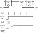
    Why do we need to synchronize signals at all? Signals arriving unrelated to the sampling clock might violate setup or hold conditions thus driving the output of the capturing flip-flop into a meta-stable state, or simply put, undefined. This means we could not guarantee the validity of the data at the output of the flip-flop. We do know, that since a flip-flop is a bi-stable device – after some (short) time the output will resolve either a logic “0” or a logic “1”. The basic idea is to block the undefined (or meta-stable) value during this settling time from propagating into the rest of the circuit and creating havoc in our state machines. The simplest implementation is to use a shift register construction as pictured

    synchro1.png

  • Uncertainty
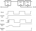
    We must remember, that regardless of the input transition, a meta-stable signal can resolve to either a logic “0” or a logic “1” after the settling time. The picture below is almost identical to the first, but here capture FF1 settled into a logic ‘0″ state. On the next clk B rising edge it will capture a static “1” value and thus change. Compare the timing of capture FF1 and capture FF2 in both diagrams. We see there is an inherent uncertainty on when capture FF2 assumes the input data. This uncertainty is one clk B period for the given synchronizer circuit.

    synchro1a.png

  • Latency
    Sometimes, the uncertainty described can hurt the performance of a system. A trick which I don’t see used so often, is to use the falling edge triggered flop as one of the capture flops. This reduces the uncertainty from 1-2 capturing clock cycles to 1-1.5 capturing clock cycles. Sometimes though, there is no meaning to this uncertainty, it becomes more meaningful when there is only a phase difference between the 2 clock domains
  • h1

    The “Bible” of Digital Design

    May 26, 2007

    This post will be very short.
    Question – What is the book on digital design?
    Answer – “CMOS VLSI design: A Circuits and Systems Perspective (3rd edition)”. If you don’t own it don’t call yourself a serious designer 🙂

    Amazon link here

    h1

    Designing Robust Circuits

    May 25, 2007

    There are many ways to design a certain circuit. Moreover, there are many trade-offs like power, area, speed etc.
    In this post we will discuss a bit about robustness and as usual, we will use a practical, real life example to state our point.

    When one talks about robustness in digital design, one usually means that if a certain type of failure occurs during operation the circuit does not need outside “help” in order to return to a defined or at least allowed state. Maybe this is a bit cryptic so let’s look at a very simple example – a ring counter.

    ring_counter_states.pngAs pictured on the right a 4 bit ring counter has 4 different states, with only a single “1” in each state. “counting” is performed by shifting or more correctly rotating the “1” to one direction with each rising clock edge. Ring counters have many uses, one of the most common is as a pointer for a synchronous FIFO. Because of their simplicity, one finds them many times in high speed full custom designs. Ring counters have only a subset of all possible states as allowed or legal states. For example, the state “1001” is not allowed.

    A very simple implementation for a ring counter is the one depicted below. The 4 flip-flops are connected in a circular shift register fashion. Three of the registers have an asynchronous reset pin while the left most has an asynchronous set pin. When going into the reset state the ring counter will assume the state “1000”.

    ring_counter1.png

    Now, imagine that for some reason (inappropriate reset removal, cross talk noise etc.) the state “1100” appeared in the above design – an illegal state. From now on, the ring counter will always toggle between illegal states and this situation will continue until the next asynchronous reset is de-asserted. If a system is noisy, and such risk is not unthinkable, hard reseting the entire system just to bring the counter to a known state might be disastrous.

    Let’s inspect a different, more robust design of a ring counter in the picture below.

    ring_counter2.png

    With the new implementation the NOR gate is functioning as the left most output. But more important, the NOR gate will drive “0”s into the 3-bit shift register until all 3-bits are “0”, then a “1” will be driven. If we look at a forbidden or illegal state like “0110”, we see that the new circuit will go through the following states: “0110”–>”0011″–>”0001″ until it independently reaches a legal state! This means we might experience an unwanted behavior for a few cycles but we would not need to reset the circuit to bring it back to a legal state.

    In a later post, when discussing Johnson counters, we will see this property again.

    h1

    Puzzle #2 – Solution

    May 23, 2007

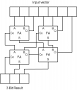
    4 full-adder units are necessary to count the amount of “1”s in a 7-bit vector.

    fa_01.png The most important thing to notice is that a full-adder “counts” the amount of “1”s of it’s inputs. If you are not convinced , then a brief look in the component’s truth table will prove this to you. The output is a binary represented 2-bit number.

    The next picture shows how to connect the four full-adders in the desired way. The first stage generates two 2-bit numbers, each represents the amount of “1”s among its respected three input bits. The second stage adds those two binary numbers together and uses the carry_in of one full-adder for the 7th bit. fa_solution.png

    As I mentioned when I posted the puzzle, I used this in an actual design. In clock and data recovery circuits (CDRs) it is necessary to integrate the amount of “ups” and “downs” a phase detector outputs (if this tells you nothing, please hold on till the CDR post I am planning). Basically, you receive two vectors of a given length, one represents “ups” the other “downs”. You have to sum up the amount of “1”s in each vector and subtract one from the other. Summing up the amount of “1”s is done using this full-adder arrangement. Another way would be using a LUT (posts on LUTs are planned as well…).

    h1

    Late Arriving Signals

    May 23, 2007

    As I mentioned before, it is my personal opinion that many digital designers put themselves more and more further away from the physical implementation of digital circuits and concentrate more on the HDL implementations. A relatively simple construction like the one I am about to discuss, is already quite hard to debug directly in HDL. With a visual aid of how the circuit looks like, it is much easier (and faster) to find a solution.

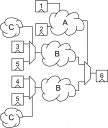
    The classic example we will discuss is that of a late arriving signal. Look at the picture below. The critical path through the circuit is along the red arrow. Let’s assume that there is a setup violation on FF6.
    late_arriving_signal_1.png Let’s also assume that in this example the logic cloud marked as “A”, which in turn controls the MUX that chooses between FF3 and FF4, is quite heavy. The combination of cloud “A” and cloud “B” plus the MUXes in sequence is just too much. But we have to use the result of “A” before calculating “B”! What can be done?

    The most important observation is that we could duplicate the entire logic that follows “A”. We assume for the duplicated blocks that one time the result of “A” was a logic “0” and in another logic “1”. Later we could choose between the two calculations. Another picture will make it clearer. late_arriving_signal_2.png
    Notice how the MUX that selected between FF3 and FF4 has vanished. There is now a MUX that selects between FF3 and FF5 (“A” result was a “0”) and a MUX in the parallel logic that selects between FF4 and FF5 (“A” result was a “1”) .
    At the end of the path we introduced a new MUX which selects between the two calculations we made, this time depending on cloud “A”. It is easy to see that although this implementation takes more area due to the duplicated logic, the calculation of the big logic clouds “A” and “B” is done in parallel rather than in series.

    This technique is relatively easy to implement and to spot if you have a circuit diagram of your design. Also do not count on the synthesis tool to do this for you. It might be able to do it with relatively small structures but when those logic clouds get bigger, you should implement this trick on your own – you will see improvements in timing (and often in synthesis run time). What you pay for is area and maybe power – nothing comes for free…

    h1

    Puzzle #1 – Solution

    May 23, 2007

    The key observation to the solution of this puzzle is to note that the outputs of components can be connected together given than only one drives a non high-Z value. If you realized that 90% of the way to solving this puzzle is behind you.

    The second step is to realize a “NOT” gate using both the “X” and “Y” components. When you know how to do that an “OR” and an “AND” gate realization are quite simple.
    The figure below sums up the construction of “NOT”, “OR” and “AND gates from various instances of “X” and “Y”.

    high-z_solution_01.png

    The next step is quite straightforward. We combine the gates we constructed and make an “XOR” gate as follows:

    high-z_solution_02.png

    This is by no means the most efficient solution in terms of minimum “X” and “Y” components.

    h1

    Do You Think Low Power???

    May 20, 2007

    There is almost no design today, where low power is not a concern. Reducing power is an issue which can be tackled on many levels, from the system design to the most fundamental implementation techniques.

    In digital design, clock gating is the back bone of low power design. It is true that there are many other ways the designer can influence the power consumption, but IMHO clock gating is the easiest and simplest to introduce without a huge overhead or compromise.

    Here is a simple example on how to easily implement low power features.

    sync_fifo.png The picture on the right shows a very simple synchronous FIFO. That FIFO is a very common design structure which is easily implementable using a shift register. The data is being pushed to the right with each clock and the tap select decides which register to pick. The problem with this construction is that with each clock all the flip-flops potentially toggle, and a clock is driven to all. This hurts especially in data or packet processing applications where the size of this FIFO can be in the range of thousands of flip-flops!!

    sync_fifo_low_power.png The correct approach is instead of moving the entire data around with each clock, to “move” the clock itself. Well not really move, but to keep only one specific cell (or row in the case of vectors) active while all the other flip-flops are gated. This is done by using a simple counter (or a state machine for specific applications) that rotates a “one hot” signal – thus enabling only one cell at a time. Notice that the data_in signal is connected to all the cells in parallel,. When new data arrives only the cell which receives a clock edge in that moment will have a new value stored.

    h1

    Your Comments Are Welcome…

    May 19, 2007

    The title of this post is self explanatory. I would be happy to get emails from you on almost any subject related to this blog.
    Let me know what you want to see, what you don’t want to see or what you want to see changed.
    My email can be found on the bottom of the about me page.