Archive for August, 2008

h1

Why You Don’t See a Lot of Verilog or VHDL on This Site

August 31, 2008

I get a lot of emails from readers from all over the world. Many want me to help them with their latest design or problem. This is OK, after all this is what this site is all about – giving tips, tricks and helping other designers making their steps through the complex world of ASIC digital design.

Many ask me for solutions directly in Verilog or VHDL. Although this would be pretty simple to give, I try to make sure NOT to do so. The reason is that it is my personal belief that thinking of a design in terms of Verilog or VHDL directly is a mistake and leads to poorer designs. I am aware that some readers may differ, but I repeatedly saw this kind of thinking leading to bigger, power hungry and faulty designs.

Moreover, I am in the opinion that for design work it is not necessary to know all the ins and outs of VHDL or Verilog (this is different if you do modeling, especially for a mixed signal project).
Eventually we all have to write code, but if you would look at my code you’d see it is extremely simple. For example, I rarely use any “for” statement and strictly try not using arrays.

Another important point on the subject is for you guys who interview people for a new position in your company. Please don’t ask your candidates to write something in VHDL as an interview question. I see and hear about this mistake over and over again. The candidate should know how to think in hardware terms; It is of far lesser importance if he can generate some sophisticated code.
If he/she knows what he is aiming for in hardware terms he/she will be a much better designer than a Verilog or VHDL wiz who doesn’t know what his code will be synthesized into. This is btw a very typical problem for people who come from CS background and go for design.

h1

Max Area = 0 ?

August 24, 2008

You are working on a design, you simulated the thing and it looks promising, first synthesis run also looks clean – jobs done right? wrong!

Many ASIC designers do not care for the area of their blocks. It has to meet the max_transition, max_capacitance and timing requirements but who cares about the area? Well if you are an engineer in soul, you should care.

I completely agree that it is a well accepted strategy not to constrain for area (or max_area = 0) when you first approach synthesis. But this doesn’t mean you should ignore the synthesis area reports, even if die size is not an issue in your project.

Not thinking about the area of your design is definitely a bad habit. Given that your transition, capacitance and timing requirements are met you should aim for lower area for your designs. In many cases the tool will meet the timing requirements at the cost of huge logic duplication and parallelism. This is OK for the critical path, but if you could do better than this for the other paths why not just “help” the tool?

For example, try thinking of pre-scaling wide increment logic or pre-decode deep logical clouds with information that might be available a cycle before. This would add some flip-flops but you might find your area decreasing significantly.

There is almost no design that can’t be improved, sometimes with a lot of engineering effort, but most designs have a lot of low hanging fruits. In my current project, I was working with one of my best engineers on optimizing some big blocks that were a legacy from another designer. In almost all blocks we were able to reduce the overall size by 30% and in some cases by over 50%!! This was not because the blocks were poorly designed, it is just that the previous designer cared less about area issues.

Bottom line – remember that smaller blocks mean:

    – Other blocks are located closer
    – Shorter wires need to be driven through the chip
    – Less hardware
    – Lower power
    – Are just more neat 🙂
h1

Arithmetic Tips and Tricks #2 – Another Look at a Slow Adder

August 18, 2008

Do you remember the old serial adder circuit below? A stream of bits comes in (LSB first) on the FA inputs, the present carry-out bit is registered and fed in the next cycle as a carry in. The sum comes in serially on the output (LSB first).

True, it is rather slow – it takes n cycles to add n bits. But hold on, check out the logic depth – one full adder only!! This means the clock can run a lot faster than your typical n-bit adder.
Moreover, it is by far the smallest, cheapest and consumes the least power of all adders known to mankind.

Of course you gotta have this high speed clock available in the system already, and you still gotta know when to stop adding and to sample your result.
Taking all this into consideration, I am sure this old nugget can still be useful somewhere. If you already used it before, or have an idea, place a comment.

h1

Real World Examples #3 – PRBS Look-ahead

August 8, 2008

PRBS generation is very useful in many digital design applications as well as in DFT.
I am almost always confused when given a PRBS polynomial and asked to implement it, so I find it handy to visit this site.

This is all nice and well for simple PRBS patterns. In some systems however, the PHY is working in a much higher rate than the digital core (say n times higher). The data is collected in wide buses in the core and then serialized (n:1 serialization) and driven out of the chip by the PHY.

This means that if we do a normal PRBS in the core clock domain, we would not get a real PRBS pattern on the pin of the chip but rather a mixed up version of PRBS with repeating sub-patterns. Best way to see this is to experiment with it on paper.

To get a real PRBS on the pin we must calculate n PRBS steps in each core clock cycle. That is, execute the polynomial, then execute it again on the result and then again, n times.

Let me describe a real life example I encountered not so long ago. The core was operating 8 times slower than the PHY and there was a requirement for a maximum length PRBS7 to be implemented.
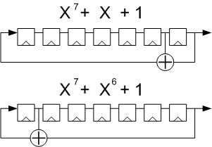
There are a few maximum length polynomials for a PRBS7, here are two of them:

Both of these will generate a maximum length sequence of 127 different states. We now have to format it into 8 registers and hand it over to the PHY on each clock, But which of the two should we use? is there a speed/power/area advantage of one over the other? does it really matter?

Well, if you do a PRBS look-ahead, which is approximately the same order as your PRBS polynomial, then it really does matter. In our case we have to do a 8 look-ahead for a PRBS 7.

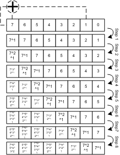
Compare the implementations of both polynomials below. For convenience both diagrams show the 8 intermediate steps needed for calculating the 8 look-ahead. In the circuit itself only the final result (the contents of the boxes in step 8 ) is used.


Because the XOR gate of the second polynomial is placed more close to where we have to shift in the new calculation of the PRBS, the amount of XORs (already too small in the second image to even notice) accumulate with each step. For the final step we have to use an XOR tree that basically XORs 7 of the 8 original bits – this is more in amount than the first implementation (even if you reuse some of the XORs in the logic) and the logic itself is deeper and thus the circuit becomes slower compared to the other implementation.

The first implementation requires at most a 3 input XOR for the calculation of look-ahead bit6 but the rest require only 2 input XOR gates.

Bottom line, if you do a PRBS look-ahead and have the possibility to choose a polynomial, choose one with lower exponents.

h1

This site is a “T-log”

August 1, 2008

I thought about it for a while and I would humbly like to introduce a new word to the English language – the word is T-log (pronounced tee-log) – a short for Technical blog. I am by the way aware that there are other uses for the acronym TLOG.

So why do I make such a big fuss about using the word “T-log” and why do I consider this site (and some others) a T-log rather than a blog?
Well, the main reason is that surfing the web for technical related blogs, you will find a lot of informative sites which deal with opinions (e.g “behind the scenes” issues, industry news or just giving their opinions on this or that topic), but the pure technical content is not there. This is actually great and this is what makes these blogs interesting to read.
However, this site is not like that. I try to give almost only technical information in the form of digital design techniques and to contribute from my own personal experience (maybe because I am too dry and can’t generate interesting posts as other bloggers do).

The bottom line is that I prefer this site not to be called a blog but rather something else – so I experiment with coining the word tlog – who knows maybe this will catch up and we will soon see a wikipedia entry… just don’t forget where you saw this first…

To wrap things up, let me recommend a cool t-log making its first steps on the web. It is run by a regular reader of this t-log who decided he also has something to say – check him out here: ASIC digital arithmetic.